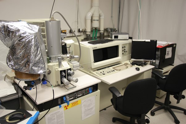
The Hitachi S-4100T is a high resolution field emission scanning electron microscope able to achieve 2 nm resolution at 30 kV. The microscope comes equipped with a Oxford Inca Energy EDS detector to obtain quantitative information regarding element distribution in a material. The operating voltage is between 0.5-30 kV.
Samples that are introduced into the chamber need to be vacuum compatible and typically conductive enough for the charge to dissipate to ground. Therefore, careful sample preparation is important for obtaining the highest quality image. Our facility comes equipped with a sputter coating system for depositing a thin metal coating on non conductive samples. In cases of semiconductors, a piece of carbon tape/copper tape may be required to dissipate charge.
